We all rely on carbon steel (CS) welds in our daily lives, whether they are on the structures we use to commute, on the pipelines that carry the fuel we use in our cars, or on the wind turbines that generate the electricity we use to prepare meals. I think we can agree that we like our CS welds strong and secure. Hence the need to inspect them for defects thoroughly and effectively.
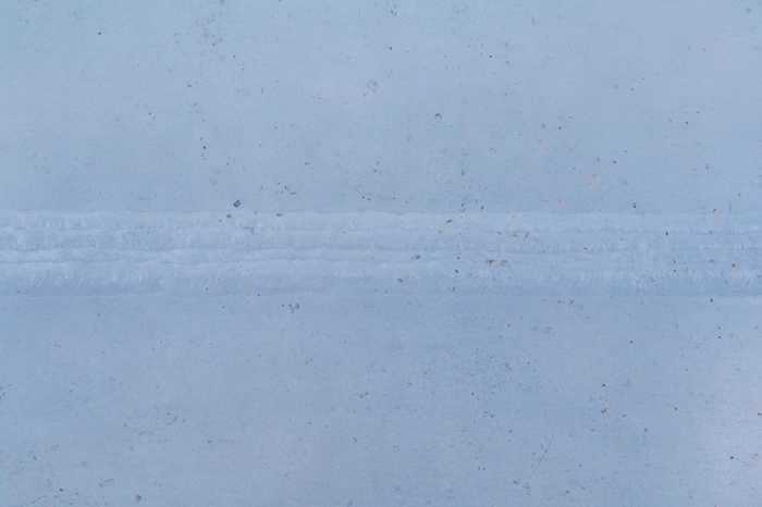
Why is that? CS is easy to weld, doesn’t cost too much, and it’s extremely reliable. But. There’s always a but. CS welds are prone to cracking and are sometimes well hidden under layers of paint and coatings used in an effort to preserve assets. The crack defects in CS welds often break their surface and are usually too small for the naked eye to see.
Furthermore, carbon steel is ferromagnetic. This means a high magnetic permeability and little to no penetration of eddy current (no skin depth).
But, we’ve never shied away from a challenge.
Conventional methods used to detect cracks in industries relying heavily on carbon steel welds include:
- Penetrant testing (PT)
- Magnetic particle testing (MT)
- ECT pencil probes
These methods require extensive and time-consuming surface preparation, the remains of which often end up released in the environment. Which adds to their high dependence on operator skills, somewhat unreliable results, inability to archive inspection data, and inherently low inspection speeds.
Another method enjoying a degree of success — electromagnetic, this time — is alternating current field measurement (ACFM®). This method relies on mathematical models to assess cracks and estimate their depth. However, while it can do what the other techniques can’t, it’s also a slow one that needs, like ECT pencil probes, several scans to cover the entire geometry of the weld while only offering partial data.
Being so widespread, but not supported properly, CS weld inspection deserved a better inspection method. To come up with it, we were faced with very interesting technological challenges:
- How do we scan the entire geometry of the weld in a single pass to speed up the inspection process?
- How do we do so without surface preparation?
- How do we achieve that with reliable positioning and depth information about crack defects?
A typical eddy current array (ECA) solution would seem, at first glance, ideally suited to this type of application. It isn’t, however. That’s because typical ECA pancake coil configurations yield signals from which it is difficult to extract depth information. Furthermore, the presence of liftoff introduces a “drift” of the operation point along this hook, which produces significant phase changes, making depth sizing impossible from a practical standpoint.
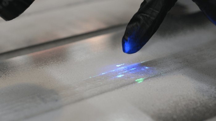
Through much R&D, we came to the conclusion that using tangential eddy current was the most promising avenue towards overcoming these challenges. As mentioned above, conventionally, the axes of pancake coils are positioned perpendicular to the surface under test. With tangential eddy current, coils are on their sides, with their axes parallel to the surface and the eddy current generated by the coil flowing parallel to the surface under test, “diving”, so to speak, under it.
So how could we use tangential eddy current and leverage the power of an eddy current array? A multiplexed ECA would solve the single-pass problem, as arrays cover a wider area. We analyzed several parameters, including coil size / impedance / position / configuration, the operating frequency, and the multiplexing pattern (topology), among others, to create an optimal ECA solution.
We tested and characterize more than 30 coil configurations over the course of a year of R&D, coming up with what we felt is the best coil configuration to leverage the power of ECA, striking a balance between coverage, penetration, and resolution. That’s how the tangential eddy current array (TECA™ ) was born.
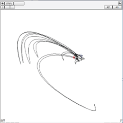
We were able to observe that TECA generated a relatively flat liftoff signal and defects approximately 90° from the liftoff signal, something that’s not possible using other inspection techniques. The multiplexed eddy current generated by TECA can dive under cracks down to 10 mm (0.4 in).
But that doesn’t take care of the geometry issue.

This was also tricky. The TECA coil design had to cover the cap, toe, and heat-affected zone of CS welds, while dynamically adjusting to the weld’s uneven geometry. The challenge lay in bundling the coils in a mechanical package that struck a balance between resolution and sizing capabilities.
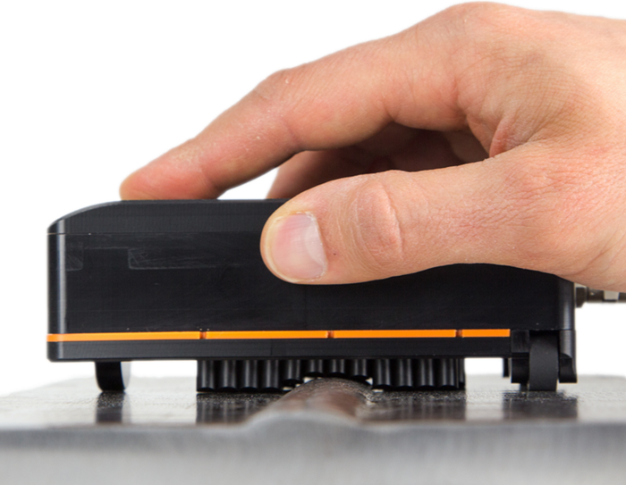
After much testing, we designed an ingenious system of independent, spring-loaded fingers that adapt to weld geometries. The individual wedged fingers all incorporate an array of coils, which provides great resolution even at higher scan speeds, surfing over the uneven geometry of the weld and enabling the a single-pass scans of entire welds.
And you would be right to ask. As I mentioned above, TECA generates a virtually flat liftoff signal, with crack-like indications approximately 90° relative to it and all the indications featuring the same phase shift.
The software processing Sharck probe data incorporates the equivalent of a three-dimensional depth-to-liftoff-to-vertical-amplitude depth plane that allows compensating for liftoff.
Add to the design a removable, high-resolution encoder and you have the final patent-pending Sharck probe capable of positioning cracks, measuring their length, and sizing them as deep as 10 mm (0.4 in), without surface preparation, at up to 200 mm/s (7.9 in/s).
Visit the Sharck probe page to find the one that suits your individual inspection needs. Also check out the Reddy® instrument, designed for portable ECA. Visit our other surface probes to find the one that fits your own special specifications.