Small-diameter pipes (in this particular application NPS 1–3) are somewhat of a challenge for pulsed eddy currents (PEC) because these pipes have highly curved surfaces and PEC probe footprints prove somewhat large for such pipes.
Nevertheless, smaller insulated pipes can benefit from PEC as much as their larger counterparts. In fact, they are subject to the same types of problems as other insulated pipes, such as corrosion under insulation (CUI) and flow-accelerated corrosion (FAC), for example. These problems can only be addressed with the methods presented in this article (radiography, for example) with the usual exception of PEC.
But using PEC on small pipes works and has several benefits.
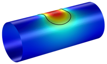
On pipes, including small pipes, the transverse PEC response is angular. As pipes get smaller, this angular response grows until pulsed eddy currents more or less “wrap” around the pipe, as you can see below.
The black line over the color-coded magnetic pulse above is the simulated emission footprint area. Pulsed eddy currents do not wrap around NPS 4 and 6 pipes, roughly covering 180° and 90°, respectively. On an NPS 2 pipe however, pulsed eddy currents completely wrap around the pipe, which suggests defects on the opposite side of the pipe could potentially be detected, albeit at a lower magnitude, because the probe is not directly centered on them.

Common belief in PEC inspections has it that a large footprint is not desirable because it yields a larger smallest detectable defect. However, a large footprint may prove to be an advantage if you’re looking for large defects; a large footprint enables screening the entire circumference of smaller pipes faster.
To illustrate, we tested the PEC response on NPS 2 pipes with gradually increasing insulation thickness (usually referred to as liftoff). Each pipe featured two simulated defects (A and B). Tests were also performed on NPS 1 and 3 pipes with similar results.
Scan Results on a Small-Diameter Pipe
Scans were performed directly over the defects (0°) and on the opposite side of the pipe, 180° from simulated defects. Here are the results.
The solid blue line represents the remaining wall thickness of defect A (when scanning directly over it) according to insulation thickness (liftoff). It displays a typical PEC behavior—as the liftoff increases, defect A fills a smaller portion of the averaging area and the capacity to accurately size defects commensurately decreases.
The dashed blue line (when scanning 180° from the defect), on the other hand, displays a different behavior. Between 0–63.5 mm (0–2.5 in), detection capabilities actually increase with liftoff—up to a point; thicker insulation decreases detection capabilities. Nevertheless, 50.8–76.2 mm (2–3 in) thick insulation clearly appears to be optimal for detection.
Here’s why. When the insulation is thin (low liftoff), the probe’s footprint is small and doesn’t wrap around the pipe. As the insulation gets thicker, the probe gradually begins to “see” the defects on the far side as the magnetic footprint begins to wrap around the pipe. Once the footprint completely wraps around the pipe, increasing the liftoff any further simply makes the footprint larger axially. The result is a growing underestimation of the defect, until the system reaches its power limit.
.png?width=535&name=MicrosoftTeams-image%20(34).png)
By running numerical simulations in conjunction with our experiments, we found the optimal conditions to detect large flaws in a single line scan—dubbed small pipe regime. As observed, it’s achieved when the footprint is large enough to enable far-side detection, while maintaining an appropriate liftoff. Of course, we also took this opportunity to characterize the limitations specific to small pipes. For the Eddyfi Lyft® probes.
On an NPS 1 pipe, with a small probe, the small pipe regime extends between liftoffs 25–38 mm (1.0–1.5 in). The optimal range with a medium probe is higher, between 38–64 mm (1.5–2.5 in), because it can tolerate more liftoff. On an NPS 2 pipe, the range shifts to 51–76 mm (2–3 in) with a medium probe. On an NPS 3 pipe, it’s over 64 mm (2.5 in) of liftoff, which is rare. Thus, in practice, the small pipe regime can only be achieved on NPS 1 and 2 pipes.
The small mass of metal and high curvature in small pipes limit the tolerance to liftoff to below specified values, as illustrated in the table above. However, this is still within typical application liftoffs.
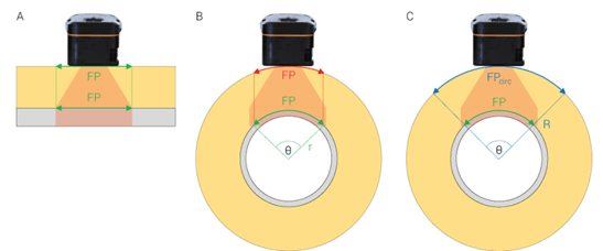
Standard PEC practices project the calculated footprint from the sample directly onto the component’s outer surface, as illustrated in panel a, below. However, when dealing with pipes, this becomes an approximation, which leads to unnecessary oversampling on pipes (panel B). To mitigate this, Lyft software version 1.2 introduces the circumferential footprint, a value used on pipes to project the footprint on the circumferential axis (panel C).
The circumferential footprint is, as you can see, larger than the actual footprint.

Now, while it’s not common practice to use pulsed eddy currents on pipes smaller than NPS 4, experimentation shows pulsed eddy currents can be used on pipes as small as NPS 1. The usual rules for footprints and smallest detectable defects are still valid, while the liftoff tolerance is somewhat limited, but remains adequate for most applications.
With sufficient liftoff on small-diameter pipes, PEC enters the small pipe regime, whereby it’s possible to screen the pipes completely in two opposed scans. (Even if you’re only looking for large defects, it’s recommended to make at least two opposed scans because defect detection and sizing is always best when defects face the PEC probe.)
The notion of circumferential footprint introduced in version 1.2 of the Lyft software—obtained empirically—enhances the system’s performance on small pipes, while screening speeds on pipes are increased 25–50 % by reducing the number of scan lines.


